Digitally controlled
FM transmitter with 2 line LCD display. (Part I)
Background
All over the net are descriptions of different types of
FM transmitters.
You can find all kinds of constructions. Some are more cryptical
than others.
One common thing about them is that they have poor explanation about function
and assembly.
Most of them don't explain the involving coils or how to make them.
How about performances and stability?
Why can't there be a construction that are easy to build and gives great
performance at the same time?
We do have been able to send people to the moon!
I finally got tired of all crap and created this page myself. A page I always
wanted to find out there.
I will show you a construction which will have great performance and still is
very easy to build.
Even if you are a fresh born homebrewer, you will be
able to follow my footsteps in this project.
I will support you with schematic , descriptions,
software, components and PCB….how about that!
Enough blurring, let's get down to business.
Project start
A transmitter needs several units to
work properly, so instead of mixing all into one huge project, I will divide
the project into 4 steps.
Each step will result in a self functional unit. In the end of this journey,
you will be able to link the steps together into a very powerful FM
transmitter.
Part I
(Digitally controlled FM transmitter with 2 line LCD display)
Part II (FM PLL controlled VCO unit)
Part III (1.5W power amplifier)
Part IV (7W power amplifier)
Part I (one)
This part will explain the main
controlling unit for the FM transmitter. This part is very important since the
transmitter frequency is digitally controlled and thereby very stable.
The hart of this unit is a PIC processor called PIC16F870, a 2 x 16 char
display and four buttons.
Let's look at the schematic now.
As you can see I have chosen a PIC16F870 because it is easy to find and cheap
to buy.
If you want more info about programming, you can look at my link:
Introduction to microcontroller PIC16F870 and PIC16F84.
If you can't find this circuit or have difficulty to program it, I can support
you with this circuit pre-programmed. Mail Me for further information.
At the schematic you will also find a 2 line 16 char display.
This display is a " HD44780-based LCD
Modules" which is very common.
Most LCD displays are based on this circuit. You will have no problem to find
it.
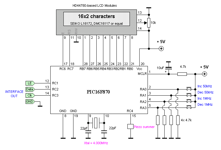
The display will show you information about the transmitting frequency.
Four wires goes to the transmitter board to control
the PLL circuit called "INTERFACE OUT", (coloured
in green left side).
When you press any of the four buttons the PIC16F870 will update both the
transmitter board and the display with new data.
The frequency of this transmitter can be changed in +/-50kHz
steps with two buttons and also in +/-1MHz steps with two other buttons.
The frequency limit is not set by software, only by the VCO of the transmitter
board.
This means that you can use this software from 0 to 999MHz, still the transmitter
board in this project will be dimensioned to work from 88 to 108 MHz.
What else do we need to say?
Well, at pin 15 you will find a piezosummer that give
a short "beep" when ever you press a button.
The PIC16F870 runs with a crystal which should be from 2 to 6 MHz….not critical
at all..
The PIC16F870 will always remember the last frequency you used and when the
power is connected, the first thing that happens is that the transmitter PLL
and display will be uppdated.
Download PIC16F870
programs (INHX8M format)
The zip file contains
hex file made for this project.
When you program the PIC16F870 there are 3 bytes in the EEPROM memory which are
interesting for you.
You can find them in EEPROM address 0, 1 and 2.
These 3 bytes set and remember the last used transmitting frequency.
If you change the frequency with the buttons, these 3 register will be updated.
In the software (transm_LCD.hex) I have made the
initial frequency is set to 90MHz.
If you wish the initial frequency to be something else than 90MHz you can easy
change the 3 bytes during programming, se table below.
|
Frequency (MHz) |
Address 0 |
Address 1 |
Address 2 |
|
88.0 |
00h |
37h |
00h |
|
89.0 |
00h |
37h |
a0h |
|
90.0 (default) |
00h |
38h |
40h |
|
91.0 |
00h |
38h |
e0h |
|
92.0 |
00h |
39h |
80h |
|
93.0 |
00h |
3ah |
20h |
|
94.0 |
00h |
3ah |
c0h |
|
95.0 |
00h |
3bh |
60h |
|
96.0 |
00h |
3ch |
00h |
|
97.0 |
00h |
3ch |
a0h |
|
98.0 |
00h |
3dh |
40h |
|
99.0 |
00h |
3dh |
e0h |
|
100.0 |
00h |
3eh |
80h |
|
101.0 |
00h |
3fh |
20h |
|
102.0 |
00h |
3fh |
c0h |
|
103.0 |
00h |
40h |
60h |
|
104.0 |
00h |
41h |
00h |
|
105.0 |
00h |
41h |
a0h |
|
106.0 |
00h |
42h |
40h |
|
107.0 |
00h |
42h |
e0h |
|
108.0 |
00h |
43h |
80h |
Option:
(If you never will change the frequency with the buttons and don't want a LCD
display, you can set the initial frequency and still use this controling circuit.)
PCB
This first part of the project involves just a PIC16F870 a display and a few
components.
It is not complicated to build and therefor I have
not made a PCB.
If many asks for a PCB I will make it and put it here.
Final word
In this part, I describes the digital controlling unit
of the transmitter.
Again, this is a strictly educational project explaining how a RF amplifier can
be built.
According to the law it is legal to build them, but not to use them.
Part II
Next part will be the RF transmitter unit.
Click here to go to FM PLL controlled
VCO unit (Part II)
FM PLL
controlled VCO unit (Part II)
Background
Many people have asked me for this project and
specially support about components and PCB.
At the bottom of this page you find all info about my support, so let's start.
All receiver and transmitter needs some kind of
oscillator.
The oscillator needs to be voltage controlled and it needs to be stable.
The easiest way to make a RF oscillator stable is to implement some kind of
frequency regulating system. Without any regulating system, the oscillator will
start to slide in frequency due to temperature shift or other influences. A
simple and common regulating system is called PLL.
I will explain it later.
 To understand this unit I suggest we
look at a block diagram at right.
To understand this unit I suggest we
look at a block diagram at right.
At the left side you find the interface from the controlling unit Part I :
Digitally controlled FM transmitter
with 2 line LCD display
There are 3 wires and ground. The 3 wires goes to the
PLL circuit.
In the right corner (Xtal) is a crystal oscillator.
This oscillator is very stable and will be the reference of the regulating
system.
The main oscillator is printed in blue and is voltage controlled.
In this construction the VCO range is 88 to 108 MHz. As you can see from the
blue arrows, some energy goes to an amplifier and some energy goes to the PLL
unit.
You can also see that the PLL can control the frequency of the VCO.
What the PLL do is that it compare the VCO frequency with the reference
frequency (which is very stable) and then regulated the VCO voltage to lock the
oscillator at desired frequency. The last part that will affect the VCO is the
audio input.
The amplitude of the audio will make the VCO change in frequnecy
FM (Frequency Modulation).
I will explain it all in detail under section Hardware and schematic.
It is not good to load or "steal" to much
energy from the oscillator because it will stop oscillating or give bad
signals.
Therefore I have added an amplifier.
The oscillator give about 15mW of energy and the following amplifier will bring
up the power to 150mW.
The amplifier can be pressed a bit more (maybe 300mW) but that is not the best
solution.
In Part III of this project I will describe a 1.5W power amplifier and in Part
IV you will find a 7W power amplifier.
For now, this unit will deliver about 150mW.
150mW doesn't sound much, but it will let you transmit RF signals 500m easy.
In one of my experiments I had 237mW output power and I could transmit 4000m in
open field using a dipole antenna.
In city environment I got 3-4 blocks. Concrete and buildings damp RF really much.
First some words about synthesiser and PLL
Before I go any future I will explain the regulating system of a PLL. Some of
you are familiar with PLL and other are not familiar.
Therefore I have copy this section from my RC receiver which explain PLL system.
(Synthesizer
and PLL can be broke down into complex regulating system with lot of math. I
hope all PLL experts have indulgence with my simplyfied
explanation below. I try to write so even fresh born homebrewers
can follow me.)
So what is a frequency synthesizer, and how does it work?
Look at the picture below and let me explain.
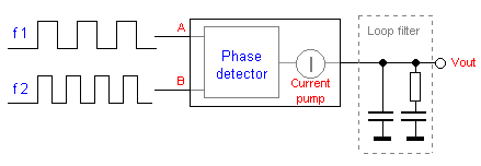
The hart of the synthesizer is something called phase detector, so let's first investigate what it does.
The picture above shows you the phase detector. It has two inputs A ,B and one
output. The output of the phase detector is a current pump. The current pump
has three states. One is to deliver a constant current and the other is to sink
a constant current. The third state is a 3-state. You can see the current pump
as a current delivery of positive and negative current.
The phase detector compares the two input frequencies f1 and f2 and you have
3 different states:
If the two
input has exact the same phase (frequency) the phase detector will not activate
the current pump,
so no current will flow (3-state).
If the phase
difference is positive (f1 is higher frequency than f2) the phase detector will
activate the current pump
and it will deliver current (positive current) to the loop filter.
If the phase
difference is negative (f1 is lower frequency than f2) the phase detector will
activate the current pump
and it will sink current (negativ current) to the
loop filter.
As you understand, the voltage over the loop filter will vary depentent of the current to it.
Okay, lets go futher and
make a Phase loocked loop (PLL) system.
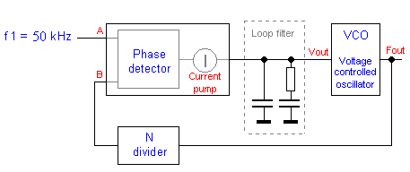
I have added a few parts to the system. A voltage controlled oscillator (VCO)
and a frequency divider (N divider) where the divider rate can be set to any
number. Let's explain the system with an example:
As you can see we feed the A input of the phase detector with a
reference frequency of 50kHz.
In this example the VCO has this data.
Vout = 0V give 88MHz out of the oscillator
Vout = 5V give 108MHz out of the oscillator.
The N divider is set to divid with 1800.
First the (Vout) is 0V and the VCO (Fout) will oscillate at about 88 MHz. The frequency from
the VCO (Fout) is divided with 1800 (N divider) and the output will be about 48.9KHz. This frequency is feeded
to the input B of the phase detector. The phase detector compares the
two input frequencies and since A is higher than B, the current
pump will deliver current to the output loop filter. The delivered current
enters the loop filter and is transformed into a voltage (Vout). Since the (Vout) start to rise, the VCO (Fout) frequency also increases.
When (Vout) is 2.5V the VCO frequency is 90 MHz. The divider divides it with 1800
and the output will be = 50KHz.
Now both A and B of the phase comparator is 50kHz and the current
pump stops to deliver current and the VCO (Fout) stay at 90MHz.
What happends if the (Vout)
is 5V?
At 5V the VCO (Fout) frequency is 108MHz and after the divider (1800) the
frequency will be about 60kHz. Now B input of
the phase detector has higher frequency than A and the current pump
starts to zink current from the loop filter and
thereby the voltage (Vout) will drop.
The reslut
of the PLL system is that the phase detector locks the VCO frequency to desired
frequency by using a phase comparator.
By changing the value of the N divider, you can lock the VCO to any frequency
from 88 to 108 MHz in step of 50kHz.
I hope this example gives you understanding of the PLL system.
In frequency synthesiser circuits as LMX-serie you can program both the N divider and the reference
frequency to many combinations.
The circuit also has sensitive high frequency input for probing the VCO to the
N divider.
For more info I suggest you download the datasheet of the circuit.
Hardware and schematic
Please look at the schematic to
follow my function description. The main oscillator is based around the
transistor Q1. This oscillator is called Colpitts oscillator
and it is voltage controlled to achieve FM (frequency modulation) and PLL
control. Q1 should be a HF transistor to work well, but in this case I have
used a cheap and common BC817 transistor which works great.
The oscillator needs a LC tank to oscillate properly. In this case the LC tank consist of L1 with the varicap
D1 and the two capacitor (C4, C5) at the base-emitter of the transistor. The
value of C1 will set the VCO range.
The large value of C1 the wider will the VCO range be. Since the capacitance of
the varicap (D1) is dependent of the voltage over it,
the capacitance will change with changed voltage.
When the voltage change, so will the oscillating frequency.
In this way you achieve a VCO function.
You can use many different varicap diod to get it working. In my case I use a varicap (SMV1251) which has a wide range 3-55pF to secure
the VCO range (88 to 108MHz).

Inside the dashed blue box you will find the audio modulation unit. This unit also include a second varicap
(D2). This varicap is biased with a DC voltage about
3-4 volt DC. This varcap is also included in the LC
tank by a capacitor (C2) of 3.9pF. The input audio will passes
the capacitor (C15) and be added to the DC voltage. Since the input audio
voltage change in amplitude, the total voltage over the varicap
(D2) will also change. As an effect of this the capacitance will change and so
will the LC tank frequency.
You have a Frequency Modulation of the carrier signal. The modulation depth is
set by the input amplitude and therefore I have added a potentiometer (P1). Now
you wonder why I don't use the first varicap (D1) to
modulate the signal?
I could do that if the frequency would be fixed, but in this project the
frequency range is 88 to 108MHz.
If you look at the varicap curve to
the left of the schematic. You can easily see that the relative
capacitance change more at lower voltage than it does at higher voltage.
Imagine I use an audio signal with constant amplitude. If I would modulated the
(D1) varicap with this amplitude the modulation depth
would differ depending on the voltage over the varicap
(D1). Remember that the voltage over varicap (D1) is
about 0V at 88MHz and +5V at 108MHz. By use two varicap
(D1) and (D2) I get the same modulation depth from 88 to 108MHz.
Now, look at the right of the LMX2346 circuit and you find the reference
frequency oscillator. This oscillator is based on the transistor (Q2) and a
crystal of 13MHz. Together they form a very stable oscillator. Most crystals
are very exact but some needs tuning. A variable capacitor (C25)
in serial with the crystal give you the ability to change the frequency
+/- a few kHz.
In most cases the crystal will be so good that you wont
need to tune it, but since I wanted high quality transmitter I implemented this
option to fine tune the reference frequency.
L2 is connected to the PLL LMX2346 circuit and will induce some of the energy
from the VCO. The PLL circuit is very sensitive so, you need only 3 to 4 turns
to get enough energy to get it working. The PLL will then use the VCO frequency
to regulate the tuning voltage.
At pin 5 of LMX2346 you will find a PLL filter to form the (Vtune) which is the regulating voltage of
the VCO.
The PLL try to regulate the (Vtune) so the VCO oscillator frequency is locked to desired
frequency.
The last part we haven't discussed is the RF power amplifier (Q3). Some energy
from the VCO is taped by (C6) to the base of the (Q3).
Q3 should be a RF transistor to obtain best RF amplification. To use a BC817
here will work, but not good.
The emitter resistor (R12) set the current through this transistor and with
R12=100 ohm and +9V power supply you will have 150mW of output power into 50
ohm load. So don't overload this poor transistor, it will be hot and burn up…
PCB

Above you can download a (pdf) filer which is the
black PCB. The PCB is mirrored because the printed side side
should be faced down the board during UV exposure.
To the right you will find a pic showing the assembly
of all components on the same board.
This is how the real board should look when you are going to solder the
components.
It is a board made for surface mounted components, so the cuppar
is on the top layer.
I am sure you can still use hole mounted components as
well.
Grey area is cuppar and each component is draw in different colours all to
make it easy to identify for you.
The scale of the pdf is 1:1 and the picture at right
is magnified with 4 times.
Click on the pic to enlarge it.
Assembly
Good grounding is very
important in a RF system. I use bottom layer as Ground and I connect it with
the top layer at several places ( five via-holes) to
get a good grounding.
Drill a small hole through the PCB an solder a wire in
each via-hole to connect the top layer with the bottom layer which is the ground
layer.
The five via-holes can easy be found on the PCB and in the assembly pic at right, they are labelled "GND" and marked with red colour.
Powerline:
Next step is to connect the power.
Add V1 (7805), C13, C14, C20, C21
Reference crystal:
Next step is to get the 13MHz reference crystal oscillator running.
Add the Xtal (13MHz), C22, C23, C24, C25, R4, R5, R6
and Q2.
Test:
Connect the main power and make sure you have +5V volt after V1.
Connect an oscilloscope or frequency meter to the emitter of Q2 and make sure
you have an oscillation of 13MHz.
If you have an accurate frequency counter you can tune the oscillator to
13.0000MHz by turning C25.
If you don't have an accurate frequency counter or any counter at all, you can
easy tune this unit later by using any FM radio receiver.
More about that later.
VCO:
Next step is to make sure the oscillator start to oscillate.
Add Q1, Q3,
L1, L3, L4,
D1, D2,
C1, C2, C3, C4, C5, C6,C7, C8, C9, C10, C11, C12, C18, C19,
R7, R8, R9, R10, R11, R12, R13, R14, R15
Now, connect a 50 ohm resistor from RF-out to ground as "dummy" load.
If you don't have a dummy load or an antenna the transistor Q3 will break easy.
When you connect the main power, the oscillator should start oscillate.
You can connect an oscilloscope to the RF output to probe the signal.
Make sure you have 3-4V DC at the junction of R13-R14.
TP is a "test point" which voltage (Vtune) will be set by the PLL circuit.
You can use this output to measure the VCO voltage to test the unit. Since the
PLL circuit hasn't been added yet, we can use this TP as input for
testing the VCO and the VCO range.
The voltage at TP will set the oscillating frequency.
If you connect TP to ground, the VCO will be oscillating at it's lowest frequency.
If you connect TP to +5V, the VCO will be oscillating at it's highest frequency.
By changing the voltage at TP you can tune the VCO to any frequency in
the VCO range.
If you have a radio in the same room you can use it to find the VCO frequency.
At this point there is no modulation of the transmitter, but you will still
find the carrier with the FM receiver.
The inductance of L1 will affect the VCO frequency and VCO range very much.
By spacing/compressing L1 you will easy change the VCO frequency.
In my test I temporary connected TP to ground and used my wireless frequency counter to check
which frequency the VCO was oscillating at. I then spaced/compressed L1 until I
got 88MHz.
Since TP was connected to ground I know 88MHz will be the lowest
oscillating frequency of the VCO.
I then reconnected TP to +5V and checked the oscillating frequency
again. This time I got 108MHz.
If you don't have a frequency counter you can use any FM radio to find the
carrier frequency.
At this point the reference oscillator works and so do the VCO.
It is time to add the last components.
PLL:
Add the LMX2346 circuit, P1, L2, C15, C16, C17, R1, R2, R3
The LMX circuit is small so you must be careful soldering it.
Extra:
It is
important that you use a dummy load of 50ohm when you test the unit.
It is
important that the varicap is mounted in right
direction (see schematic).
It is
important that you are careful and accurate when you solder the componets.
Make sure you
don't have any tin/lead bridges which short-circuit strip-lines to ground.
The RF unit is now ready to be connected to the Digitally controlled FM transmitter with 2 line LCD display
Component support
This project has be constructed to use standard (and easy to find) components.
People often write to me and ask for components, PCB or kits for my projects.
This is the only project I can offer you a start kit for a small fee.
|
The kit cost 15 Euro (18 USD) and includes: 1 PCB (etched and drilled vias) 2 Varicap
(sm1251) 1 Reference crystal (very accurate
and match PCB) 1 PLL circuit 2 wires for the air coils 1 BFR 93 NPN transistor 2 BC817-25 NPN transistor 1 variable capacitor C25 2 100k ohm (0603 size) works equal
good 2 100 ohm (0805 size) 10 100nF (0603 size) works equal
good |
Final word
This part II describes the FM PLL controlled VCO unit.
Again, this is a strictly educational project explaining how a RF amplifier can
be built.
According to the law it is legal to build them, but not to use them.
Part III
Next part will be the 1.5W Power amplifier unit.
It will soon be
presented on my homepage.
1.3W Power Amplifier (Part III)
Background
Some amplifier is based around a RF
transistor.
In my case I will use a common NPN RF transistor called 2SC1970.
You can also use other transistors like 2N4427 and some others.
Check datasheets to se how much power the transistor can handle.
2SC1970 will handle 1.3W and 2SC1971 up to 6W.
Most transistor has a power gain of 10dB meaning 10
times power amplification.
This is the reason why you must use several stages to achieve a strong
transmitter.
In this construction we are getting higher power then ever and you must be
careful with the transistor.
A 50 ohm dummy load MUST be used while testing, else
the final transistor will break.
An antenna can be used but the antenna must be properly made else the transistor
will break.
More about that later.
Hardware and schematic
In all RF system and specially in RF
amplifiers, it is very important to have a stable power supply and making sure
you won't get any RF out on the power line. The Capacitor C12 and C13 will stabilise the DC power supply. L1, C10, C11 and L3 with C8,
C9 will also prevent RF from leaking out to the powerline
and cause oscillation or disturbances. L1 and L3 should be ferrite chokes or
inductance's about 1 to 10 uH.
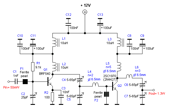
Transistor Q1 will act as a buffer amplifier, because I don't want to load the
previous stage to much.
The input RF signal is passin C1 and F1 which is a
small ferrite pearl where the wire just passing through.
F1 with C2 will act as an impedance matching for Q1.
F1 can be substituted with a coil as L4, but in my test I found that the
ferrite pearls gave best performances.
L2 is nit a critical component and any coil from 2-10uH will do the job. Q1
will amplify the input signal from 50mW to about 200mW.
Q1 can amplify much more, but It doesn't need to do
that because 200mW is good for the final transistor.
If you want higher power you can decrease the resistor R2.
If you look at Q2 you will also find a ferrite pearl F2 at the base to emitter.
This ferrite pearls is to set the DC voltage to zero and be a high impedance
for RF signals. I wounded the wire 4 times around this small ferrite pearl. You
can substitute it with a coil of 1uH or more.
C4, C5 and L4 forms an input matching unit for the
transistor. Not much we can do about that…
At the output of the final transistor Q2 you will find 2 coils L5 and L6.
Together with C6 and C7, they form an impedance unit for the antenna and also
for the transistor.
PCB

Above you can download a (pdf) filer which is the
black PCB. The PCB is mirrored because the printed side side
should be faced down the board during UV exposure.
To the right you will find a pic showing the assembly
of all components on the same board.
This is how the real board should look when you are going to solder the
components.
It is a board made for surface mounted components, so the cuppar
is on the top layer.
I am sure you can still use hole mounted components as
well.
Grey area is cuppar and each component is draw in different colours all to
make it easy to identify for you.
The scale of the pdf is 1:1 and the picture at right
is magnified with 4 times.
Click on the pic to enlarge it.
RF power
This amplifier is based on the
transistor 2SC1970 and 2N4427.
The output power is about 1.3W and the input driving power is 30-50mW.
You can use other transistor as 2SC1971 and get much more output power.
1.3W will still get your RF signal quit far and I advice you to use a good 50
ohm resistor as dummy load.
Make sure it can take up to 5-10W, else it will be a hot resistor.
You MUST use an antenna or 50 ohm dummy resistor while testing else you
burn up the transistor.
RF power
As you can see there are several
variable capacitor and coils in this construction and it must be so.
I advice you to put all in middle range before you apply power.
To tune this amplifier you can either use a wattmeter, SWR unit or you can do
as I do using a RF field meter.
Assembly
Good grounding is very important in a RF
system.
I use bottom layer as Ground and I connect it with the top with wires to get a
good grounding.
Make sure you have some cooling at the transistor.
In my case I put the 2SC1970 close to the PCB to handle the heat.
With good tuning the transistor shouldn't become hot.
Component support
This project has be constructed to use standard (and
easy to find) components.
People often write to me and ask for components, PCB or kits for my projects.
I can offer you PCB for a small fee. Click here to mail me for more information
about kit.
I can support you with some components, Click here for more info.
Low pass filter
Some of you might want to add a low-pass filter at the output.
I have not added any extra low pass filter in my construction because I don't
think it is needed.
You can easy find several homepages about low pass filter and how to build
them.
I will not go future into this subject.
Final word
This part II describes the FM PLL controlled VCO unit.
Again, this is a strictly educational project explaining how a RF amplifier can
be built.
According to the law it is legal to build them, but not to use them.
Part IV
Next part will be the 7W (or maybe more) Power amplifier unit.
Если кому ни будь нужна прошивка на микроконтроллер
пишите мне на Email: evg-bubnov@yandex.ru .