Усилитель мощности на 40 ватт.
Performance summary
|
Suggested Rough and Ready
Construction Procedure
- Cut out a piece of double sided PCB material for the main board (approx. 100 x 85mm)
- Create the aperture for the FET, using a
selection of drills and files. Use the FET as a template, if
required, but don't blow it up with static. Make sure you'll end up
with the drain on the right side.
- Drill six holes in the PCB, these are to
hold the PCB to the diecast box
- Place the PCB in the box and use the holes
in the PCB to drill through the box
- Temporarily screw the PCB to the box
- Work out where the heatsink
is going to go, underneath the box The
device should end up towards the centre of the heatsink.
Either drill some more holes through the whole
lot, and re-use some of the existing PCB/box holes and extend these down
through the heatsink. Temporarily screw
the heatsink to the PCB/box assembly. When
you look into the top of the box you should now see a piece of heatsink revealed, the same size as the base of the
FET.
- Rig yourself up some static protection (if
you've got an old blown-up device or a bipolar device in the same package
you won't have to bother with this) and drop the device into the aperture
in the board.
- Use the FET to give you give the centre positions
of its' mounting holes
- Take everything to bits again. Make
two holes in the heatsink for the FET
- Drill the holes in the two ends of the box
for the RF connectors and the feedthrough
capacitor
- Tin the PCB, top and bottom, with a big
iron. Use just enough solder to get a smooth finish but not too much
to create raised areas of solder, especially on the bottom, as these will
prevent the PCB sitting flat against the box floor.
- Create the two islands for the FET gate
and drain, as detailed in the above paragraph
- Solder copper tape between top and bottom
faces of the PCB underneath where the source tabs will be
- Create the PCB islands, tin them, stick
them on the PCB using the photograph as a guide
- Create and fit the screen between the
amplifier and the LPF areas
- Fit all the remaining PCB components, with
the exception of the FET
- Fit the PCB to the box and the heatsink
- Fit the and connect and the RF connectors
and the feed-through capacitor
- Taking anti-static precautions again, apply the thinnest continuous film possible of heat transfer paste to the base of the FET. This can be conveniently done with a wooden cocktail stick
- Bend up the last 2mm of each of the FET's leads. This will make it much easier to
remove, should the need arise
- Screw the FET to the heatsink.
Too loose and the device will over-heat, too tight and you will distort
the flange of the device and once again it will overheat. If you've
got a torque screwdriver, look up the recommended torque and use it.
- If you've understood the instructions
correctly, the tabs of the device will be fractionally above the PCB Solder the FET in with the big iron, first the
sources, then the drain, finally the gate. You may have to
disconnect L4 and L5 while you are fitting the FET, but don't disconnect
R3 as this provides static protection for the device.
Schematic
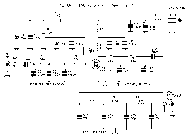
Parts List
|
Reference |
Description |
FEC Part No. |
Quantity |
|
C1, C2, C4 |
5.5 - 50p
miniature ceramic trimmer (green) |
148-161 |
3 |
|
C3 |
100p
ceramic disc 50V NP0 dielectric |
896-457 |
1 |
|
C5, C6, C7 |
100n
multilayer ceramic 50V X7R dielectric |
146-227 |
3 |
|
C8 |
100u 35V
electrolytic radial capacitor |
667-419 |
1 |
|
C9 |
500p
metal clad capacitor 500V |
|
1 |
|
C10 |
1n
ceramic lead through capacitor capacitor |
149-150 |
1 |
|
C11 |
16 - 100p
mica compression trimmer capacitor (Arco 424) |
|
1 |
|
C12 |
25 - 150p
mica compression trimmer capacitor (Arco 423 or Sprague GMA30300) |
|
1 |
|
C13 |
300p
metal clad capacitor 500V |
|
1 |
|
C14, C17 |
25p metal
clad capacitor 500V |
|
2 |
|
C15, C16 |
50p metal
clad capacitor 500V |
|
2 |
|
L1 |
64nH
inductor - 4 turns 18 SWG tinned Cu wire on 6.5mm dia.
former, turns length 8mm |
|
1 |
|
L2 |
25nH
inductor - 2 turns 18 SWG tinned Cu wire on 6.5mm dia.
former, turns length 4mm |
|
1 |
|
L3 |
6 hole
ferrite bead threaded with 2.5 turns 22 SWG tinned Cu Wire to form wideband
choke |
219-850 |
1 |
|
L4 |
210nH
inductor - 8 turns 18 SWG enamelled Cu wire on
6.5mm dia. former, turns length 12mm |
|
1 |
|
L5 |
21nH
inductor - 3 turns 18 SWG tinned Cu wire on 4mm dia.
former, turns length 10mm |
|
1 |
|
L6 |
41nH
inductor - 4 turns 22 SWG tinned Cu wire on 4mm dia.
former, turns length 6mm |
|
1 |
|
L7 |
2 ferrite
beads threaded onto lead of C10 |
242-500 |
2 |
|
L8, L10 |
100nH inductor
- 5 turns 18 SWG tinned Cu wire on 6.5mm dia.
former, turns length 8mm |
|
2 |
|
L9 |
115nH
inductor - 6 turns 18 SWG tinned Cu wire on 6.5mm dia.
former, turns length 12mm |
|
1 |
|
R1 |
10K cermet potentiometer 0.5W |
108-566 |
1 |
|
R2 |
1K8 metal
film resistor 0.5W |
333-864 |
1 |
|
R3 |
33R metal
film resistor 0.5W |
333-440 |
1 |
|
D1, D2 |
BZX79C5V6 400mW Zener Diode |
931-779 |
2 |
|
TR1 |
MRF171A (Motorola) |
|
1 |
|
SK1 |
BNC bulkhead socket |
583-509 |
1 |
|
SK2 |
N type
panel socket, square flange |
310-025 |
1 |
|
|
|
|
|
|
|
Diecast
|
301-530 |
1 |
|
|
Heatsink
16 x 60 x 89mm 3.4°C/W (Redpoint Thermalloy 3.5Y1) |
170-088 |
1 |
|
|
Double
sided Cu clad PCB material 1.6mm thick |
|
A/R |
|
|
Copper Tape or Foil |
152-659 |
A/R |
|
|
M3 nut,
bolt, crinkly washer set |
|
16 |
|
|
Non-Silicone
Heat Transfer Paste |
317-950 |
A/R |
Notes
- Farnell Part Numbers are for guide
only - other equivalent parts can be substituted.
- Metal clad capacitors are either MCM series, Unelco
J101 series, Underwood, or Arco MCJ-101 series available from,
amongst other places, RF Parts.
- MRF171A available from BFI (UK),
Richardson or RF Parts (US)
- Arco or Sprague trimmers are available
from Communication Concepts (US)
- 18 SWG (standard wire gauge) is
approximately 1.2mm diameter
- 22 SWG (standard wire gauge) is
approximately 0.7mm diameter
- To make the inductors - wind the required
number of turns round an appropriately sized former, initially use one
wire diameter spacing between each turn. Then pull the turns apart
to get the length required in the parts list table. Finally check
the value using a network analyser and adjust
accordingly.
- The exception to the above spacing rule is
L4, which is close wound.
- Copper foil is available from craft shops
(used in stained glass making)
- A/R = as required
Photograph of Prototype Amplifier

Note orientation of the FET. The lead with the
slash is the drain, and is to the right